
Elon Musk's bet on a particle accelerator to print chips
No filing describes the system and no lab has shown it printing chips at fab scale, leaving the Dutch company's tin-plasma machines the only production option for years even at Terafab's proposed size.


What happenedA 6 August reply reading 'FEL FTW' to a fan guess about a circular structure in a SpaceX render of the planned Texas Terafab was taken as confirmation the campus will use accelerator-based light instead of ASML's machines, though no SpaceX or Tesla filing describes such a system.
Why it mattersA working accelerator source could in theory cut energy per wafer, avoid tin debris and reach shorter wavelengths for future chips, but no lab has yet printed a chip with it and near-term supply still runs through ASML alone.
Still openWhether the post was a Terafab design choice or just a general preference, and whether an accelerator can deliver stable, round-the-clock light to dozens of scanners without loss, contamination or single-point failure.
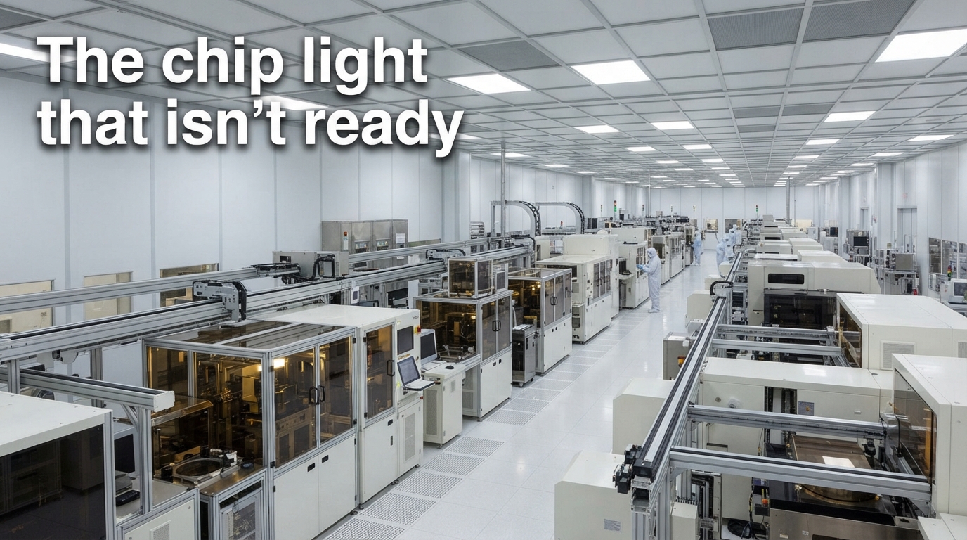
Musk's two-word chip bet and why the physics is easier than the factory
On 6 August 2026 Elon Musk replied "FEL FTW (free-electron laser, for the win)" to speculation on X that a SpaceX night render of the planned Texas Terafab showed a particle-accelerator ring, sparking claims the giant chip campus will ditch ASML machines for a different kind of light. It is a two-word preference signal, not a factory plan no SpaceX or Tesla filing describes such a system and even if it were a plan, the technology it points to, free-electron laser EUV lithography a particle-accelerator alternative to ASML's tin-plasma light source for printing chips has never printed a chip in a fab.
What FEL promises vs what ASML's machines actually do today — power, energy per scanner, and cost. Side-by-side per-scanner comparison of ASML’s production laser-produced plasma (LPP) EUV source versus free-electron laser (FEL) projections: LPP delivers 500 W of usable EUV on about 1.1 MW wall-plug draw, while FEL advocates claim 2,000 W per scanner on about 0.5 MW (a 4 MW site feed shared across eight scanners) — roughly four times the light at half the energy. Those FEL bars are lab and industry projections only; no FEL has exposed production wafers, and the more efficient Nb₃Sn cavity path (about 2 MW total for eight scanners) is also unproven at fab scale. ASML’s tools that use today’s LPP sources start around USD 220M for low-NA EUV and more than USD 400M for High-NA; the company shipped 48 EUV systems in 2025. — AI-assisted analytic, built only from real cited or sourced data. Source: 36Kr (English), IEEE Spectrum, Optics & Photonics News (Optica). As of 2026-08-10.
The physics behind the idea is attractive on paper, and at Terafab's proposed scale the economics would look better than anywhere else. But the engineering to make it run 24 hours a day, without contaminating or starving dozens of scanners, does not exist yet. Chipmaking will run through ASML for years regardless of what Musk prefers.
What was actually said and what wasn't
The entire narrative traces to two artifacts on the same day. SpaceX posted a night render video of Terafab, the planned semiconductor campus in Grimes County, Texas. Viewers noticed a large circular structure and guessed it was a synchrotron ring for a free-electron laser. The account @beffjezos Beff Jezos, who runs the AI hardware startup Extropic posted that guess. Musk, who leads SpaceX and Tesla, replied "FEL FTW" at about 4:28 p.m. ET on 6 August 2026.
That is what is verifiable. What is not verifiable is any commitment. The SpaceX Updates page that announced Terafab "Breaking Ground on Terafab in Texas" and the Texas filings that authorized it, including the Texas Enterprise Fund $30 million grant and the Jobs, Energy, Technology and Innovation (JETI) qualification, mention no free-electron laser. No SpaceX, Tesla or xAI press release, SEC filing, patent or technical paper describes a beam energy, undulator period, power target or distribution optics for Terafab.
Secondary explainers including OfficeChai, China's 36Kr, and Dealroom treated the reply as confirmation that "Terafab will use FEL rather than conventional EUV." That upgrades a preference to a plan. The responsible reading is narrower: Musk signaled he favors free-electron lasers. Whether he meant Terafab specifically, or the technology in general, is not settled in the primary post, and the timestamp and exact context have not been independently verified from the X post itself beyond secondary quotations.
Where FEL-EUV actually is on the road to a fab — and when Terafab says it will need it. Horizontal timeline of free-electron-laser EUV milestones from 2011 through 2030, as of 10 August 2026. The only lab demonstration on the chart is KEK's April 2023 infrared SASE run (20 μm at 17 MeV) — not EUV — while xLight's Albany prototype is still a 2028 target and Terafab mass production in 2029 is a filing projection; Musk's 6 August 2026 "FEL FTW" reply is signal only, not a technical demonstration. Quiet years 2011–2019 are compressed so the post-2023 funding and claims remain readable. — AI-assisted analytic, built only from real cited or sourced data. Source: 36Kr (English), IEEE Spectrum, Optics & Photonics News (Optica). As of 2026-08-10.
What Terafab is and isn't yet
Terafab is not a fab. It is a planned, vertically integrated campus logic plus memory plus advanced packaging and testing under one roof at the former Gibbons Creek coal plant site in Grimes County, between Houston and College Station. SpaceX and Tesla, with xAI and with Intel providing its 18A/14A process nodes (its next-generation transistor manufacturing recipes) and EMIB/Foveros packaging (methods for stacking and connecting chips), as a domestic alternative to TSMC's CoWoS (its competing chip-stacking method), say they need it because their combined demand for AI compute will exceed 1 terawatt, far beyond current global supply.
The scale is why the FEL idea keeps coming up. SpaceX and the state of Texas describe more than 100 million square feet of manufacturing space, with an initial phase of about $16.8 billion and at least 3,000 jobs, supported by a $30 million Texas Enterprise Fund grant and JETI qualification. The Houston station KHOU, reporting Gov. Greg Abbott's announcement, and Reuters, reporting SpaceX's own statement that day, both put the first phase at $16.8 billion and 3,000 jobs for a 100-million-square-foot vertically integrated plant making, packaging and testing logic and memory chips. Abbott said the "first-of-its-kind Terafab facility will accelerate chip production in Texas at an unprecedented scale," while Musk said it would combine logic, memory and advanced packaging to produce AI chips "at scale for use on Earth and in space."
Broader filing-derived projections put a first-phase estimate at $55 billion and a full build at $119 billion, with construction from 2026 to 2037 and mass production targeted for 2029. Reuters reported that a May filing showed SpaceX had proposed $55 billion initially, rising to $119 billion if extra phases complete, and 36Kr, summarizing SpaceX filings, reported the same $16.8 billion first phase, over 100 million square feet (about 9.29 million square meters), an 11-year window to 2037, mass production in 2029, and a long-term total up to $119 billion. Those are projections, not committed capex. 36Kr also detailed the site logic: the Gibbons Creek Reservoir, used for decades to cool the coal plant decommissioned in 2019, would supply rainwater and surface water for closed-loop recycling with on-site treatment, avoiding groundwater pumping, and an on-site natural gas plant would power the campus off the Texas grid. Musk has shared a size comparison showing the main building about 2.5 miles long and roughly 50 times the Pentagon, in four giant buildings.
The site is pre-construction. Tesla broke ground in April on a smaller research fab at the North Campus of its Giga Texas plant as a precursor, a $3 billion pilot built around Intel technology to test process recipes before the main campus is ready, according to both Reuters and 36Kr. Terafab has no announced ASML EUV order. ASML chief executive Christophe Fouquet confirmed in May 2026 that he had talked directly with Musk "He's very serious" but noted the market is supply-limited. That matters for the FEL stakes: a centralized light source only helps if you are building at a scale where one accelerator feeding many scanners amortizes its cost. Terafab, if built as described, would be that scale. Today it is a plan with a location and incentives, not a customer in ASML's backlog.
How EUV light is made and why an accelerator looks better on paper
EUV lithography light with a 13.5-nanometer wavelength used to print the tiniest transistor patterns works because shorter wavelength means smaller features. Making that light is the hard part.
ASML, the Dutch company that is the sole maker of production EUV machines, does it with laser-produced plasma, or LPP. A CO2 laser fires at molten tin droplets about 50,000 times per second, first reshaping then vaporizing each droplet into plasma hotter than 200,000C. The plasma emits EUV, which multilayer mirrors collect and filter to 13.5 nanometers and guide through vacuum to the scanner. It is one light source per scanner, broadband and unpolarized, with wall-plug efficiency below 0.1%. It needs about 600 liters of hydrogen per minute to keep tin debris off the collector mirror, and that mirror still degrades and must be replaced a major operating cost. Stochastic defects random pattern errors when too few photons arrive get worse as features shrink, so more power is always needed.
A free-electron laser, or FEL, makes EUV differently. An electron gun injects electrons into a superconducting linear accelerator that pushes them to near light speed about 1 GeV, or a Lorentz factor near 1,000 then sends them through an undulator, a row of alternating magnets with centimeter-scale period. The electrons wiggle, emit light, and through self-amplified spontaneous emission (SASE) they bunch into microbunches spaced one wavelength apart that radiate coherently. The wavelength follows bbr = bbu / 2b3 (1+K/2), so tuning the beam energy tunes the color. There is no tin, no gain medium to damage, and the light is coherent, polarized and narrow-band. One accelerator can feed many scanners through mirrors, like a utility.
On paper the advantages stack up. Proponents including the U.S. startup xLight and the Optica review that laid out the physics project 2,000 watts to eight scanners on 4 megawatts total, versus 500 watts on 8.8 megawatts for eight LPP sources, and as low as 2 megawatts if niobium-tin (Nb3Sn) cavities replace pure niobium. KEK, the Japanese High Energy Accelerator Research Organization in Tsukuba, estimates 1/4 to 1/5 the energy per EUV watt. There is no tin debris or collector wear, the light is polarized useful for high-numerical-aperture imaging where contrast depends on polarization and the wavelength can be tuned to about 6.7 nanometers for beyond-EUV nodes, avoiding the need to swap tin for toxic gadolinium that LPP would require at that wavelength.
None of those numbers are measured fab results. They assume an energy-recovery linac that recycles beam energy and Nb3Sn cavities that have not been proven at fab scale. LPP is also improving: ASML has a roadmap to 1,000-watt sources, throughput around 200 wafers per hour, and alternative drive lasers such as thulium-doped YLF at 1.9 microns versus CO2 at 10.6 microns to improve efficiency. The FEL has to beat a moving incumbent.
No one has shown it working for chips
No group has demonstrated FEL-EUV lithography at production relevance. The field is at lab-to-prototype transition, not fab-ready.
Japan's KEK built its compact energy-recovery linac, or cERL, between 2011 and 2013 and modified it in 2019-20 to test the idea. It has generated SASE light but at 20-micrometer infrared at 17 MeV, published in April 2023, not at 13.5-nanometer EUV. Reaching EUV requires an 800 MeV upgrade with new superconducting cavities, a new electron gun and new undulators, beyond the existing hall. In 2021, before recent inflation, KEK estimated construction excluding land at 40 billion yen about $260 million at the time for 10 kilowatts of EUV to multiple tools, plus about 4 billion yen a year to run. The machine lives in a 60-meter by 20-meter all-concrete room for radiation shielding.
In the United States, xLight, the Palo Alto startup whose executive chairman is former Intel chief Pat Gelsinger, has not yet built a prototype. It received a non-binding letter of intent in December 2025 for up to $150 million in CHIPS Act incentives, finalized on 2 June 2026 as a $150 million award from the Commerce Department's CHIPS Research and Development Office and NIST, the U.S. National Institute of Standards and Technology, which oversees CHIPS R&D, with $150 million in equity to the government. The money is for construction and demonstration of a first-of-its-kind FEL prototype at the Albany NanoTech Complex in New York, with NYCreates, beginning in 2028, to be integrated with ASML scanners and to pioneer sub-EUV research. That is a demonstration, not a production-qualified source. Other efforts Substrate, Tau Systems with laser-wakefield approaches are similarly pre-commercial.
ASML itself evaluated FEL light sources a decade ago and again more recently when comparing FEL progress to the LPP roadmap, and chose LPP. That revealed preference is part of the evidence.
Why superior physics hasn't become a product
The obstacles are not details to work out. They are the reason a technology researched since the 1990s has not shipped.
Scale and cost come first. An accelerator plus undulator plus shielding is a synchrotron-scale facility, hundreds of millions upfront, versus a modular LPP source per scanner that a fab can add incrementally.
Stability is second. A fab needs 24/7 uptime; any jitter in beam energy or position imprints directly on wafer yield. Lab stability is not industrial stability. Independent experts interviewed by IEEE Spectrum put it bluntly. Ahmed Hassanein, who leads the Center for Materials Under Extreme Environment at Purdue University, said the R&D roadmap "will involve numerous demanding stages in order to develop a reliable, mature system" requiring "serious investment and take considerable time." Stephen Benson, recently retired senior research scientist at Jefferson Lab, said the machine "must be extremely robust, with redundancy built in" and ensure components are not damaged from radiation or laser light "without compromising performance, which must be good enough to ensure decent wall-plug efficiency." Benson warned that without forthcoming investment, "development of EUV-FELs might not come in time to help the semiconductor industry."
Radiation and vacuum are third. GeV electrons produce intense radiation requiring heavy shielding; the beam runs in vacuum.
Transport is fourth. EUV does not travel in air. Getting light from a central FEL to dozens of scanners tens of meters away means grazing-incidence mirrors with loss and contamination risk. KEK's own design notes pulse energy density around 10 millijoules per square centimeter at 3 meters, approaching the ablation threshold of molybdenum-silicon mirrors around 20 millijoules per square centimeter, requiring beam expansion with curved mirrors to stay safe.
Redundancy is fifth. A single central source is a single point of failure: one FEL down takes about ten scanners down. A fab would need near-100% availability and duplicate FELs. That is why ASML's choice of LPP more modular, fewer systemic risks has held.
The efficiency gains that make FEL attractive also depend on unproven pieces: an energy-recovery linac operating at high current and Nb3Sn cavities at scale. Without them, the power math does not close.
What it would mean if it worked and why it means nothing for supply yet
There are two time horizons, and they point opposite ways.
If FEL-EUV were industrialized at fab-grade reliability, it would be the first credible alternative light source to ASML's 100% monopoly on production EUV. ASML shipped 48 EUV systems in 2025 EUV sales ac11.6 billion within total net sales of ac32.7 billion and net income of ac9.6 billion, with Q4 bookings of ac13.2 billion (ac7.4 billion EUV) and a backlog of ac38.8 billion. A standard low-NA tool costs about $220 million, a High NA EXE:5200B more than $400 million. A working FEL would offer roughly four times the power at half the energy, no tin debris or hydrogen curtain, tunable wavelength to 6.7 nanometers for sub-nanometer nodes, and lower operating cost once the high capex is amortized. For Terafab, which talks about 1 terawatt a year by some estimates 22.4 million wafers a year, multiples of current global DRAM output centralized economics improve with scale: the bigger the fab, the better a utility model looks. That is the bull case, and it fits Musk's pattern of vertically integrating and rebuilding from first principles, as with rockets and batteries.
The near term is established and different. Terafab is a prospective customer with no orders, in a market where backlog is allocated through 2027 to TSMC, Samsung and Intel. Even xLight's 2028 demo, if on time, is not a product, let alone a qualified source that a fab would bet a $16.8 billion first phase on without an ASML fallback. ASML's monopoly is structural today, and Terafab's scale if it materializes makes it a huge buyer before it could ever be a competitor.
In that sense "FEL FTW" is best read as exactly what it says: for the win, in principle. The physics win is real enough that Japan and the United States are spending public money to test it. The factory win would require proving that a particle accelerator can run like a light bulb always on, always stable, always clean and that EUV can be piped like water to a hundred scanners without loss. No one has shown that. Until someone does, the lights in any Terafab that gets built will still depend on tin droplets and CO2 lasers, one scanner at a time.
Source recordSources / claims / limits
How this piece is framed: Signal vs. substance: a two-word preference signal inflated into a factory plan, measured against the real physics promise and the industrialization gap of FEL-EUV
Charts & tables — AI-assisted; provenance on each line
- FEL claims 4x the light at half the energy — but none of it has printed a chip — sourced for this figure · as of 2026-08-10
- No production FEL-EUV exists — the first demo is still two years away — from claims clm_8d2627efef, clm_85c1828262, clm_64c06e0c11, clm_235ca61ce8, clm_88bb4901e6, clm_b5e0a48bb3 · as of 2026-08-10
Sources
- (primary) Breaking Ground on Terafab in Texas — SpaceX Updates — https://www.spacex.com/updates · read in full · captured 2026-08-10
- (primary) Department of Commerce and NIST Announce CHIPS Research and Development Letter of Intent with xLight — NIST / U.S. Department of Commerce — https://www.nist.gov/news-events/news/2025/12/department-commerce-and-nist-announce-chips-research-and-development-letter · read in full · captured 2026-08-10
- (primary) ASML reports 32.7 billion total net sales and 9.6 billion net income in 2025 — https://www.asml.com/en/news/press-releases/2026/q4-2025-financial-results · read in full · captured 2026-08-10
- (primary) SpaceX to build $16.8 billion semiconductor plant in Grimes County — KHOU 11 / Gov. Greg Abbott statement — https://www.khou.com/article/news/local/grimes-county-texas-spacex-plant/285-77593643-b7d1-4eaf-9a4a-a3f1534abd0e · read in full · captured 2026-08-10
- (primary) Department of Commerce Announces Finalization of CHIPS Incentives with xLight to Support Next-Generation Light Source for Lithography — NIST / U.S. Department of Commerce — https://www.nist.gov/news-events/news/2026/06/department-commerce-announces-finalization-chips-incentives-xlight-support · read in full · captured 2026-08-10
- (primary) Governor Abbott Announces SpaceX Expansion In Grimes County — State of Texas — https://gov.texas.gov/news/post/governor-abbott-announces-spacex-expansion-in-grimes-county · read in full · captured 2026-08-10
- (primary) ASML CEO sees tight supply in booming chip market as AI demand soars — Reuters — https://www.reuters.com/business/autos-transportation/asml-ceo-sees-tight-supply-booming-chip-market-ai-demand-soars-2026-05-20/ · read in full · captured 2026-08-10
- (secondary) SpaceX, Tesla to initially spend $16.8 billion on Terafab chip plant in Texas — Reuters — https://www.reuters.com/business/media-telecom/spacex-says-terafab-be-built-texas-with-initial-investment-168-billion-2026-08-06 · read in full · captured 2026-08-10
- (secondary) Elon Musk addresses ASML employees, pushes into chip manufacturing — CNBC — https://www.cnbc.com/2026/06/11/elon-musk-addresses-asml-employees-pushes-into-chip-manufacturing.html · read in full · captured 2026-08-10
- (secondary) Exclusive look at High NA, ASML's new $400 million chipmaking colossus — CNBC — https://www.cnbc.com/2025/05/22/exclusive-look-at-high-na-asmls-new-400-million-chipmaking-colossus.html · read in full · captured 2026-08-10
- (secondary) EUV Light Source: Is the Future in a Particle Accelerator? — IEEE Spectrum — https://spectrum.ieee.org/euv-fel · read in full · captured 2026-08-10
- (secondary) Elon Said "FEL FTW." Here's the Laser That Will Boost Chip Volumes 50X — NextBigFuture — https://www.nextbigfuture.com/2026/08/elon-said-fel-ftw-heres-the-laser-that-will-boost-chip-volumes-50x.html · read in full · captured 2026-08-10
- (secondary) FELs and the Future of Lithography — Optics & Photonics News (Optica) — https://www.optica-opn.org/home/articles/volume_36/november_2025/features/fels_and_the_future_of_lithography · read in full · captured 2026-08-10
- (secondary) ASML faces a double-edged Terafab: prospective customer and potential EUV rival — Dealroom — https://app.dealroom.co/news/note/asml-faces-a-double-edged-terafab-prospective-customer-and-potential-euv-rival · read in full · captured 2026-08-10
- (secondary) "FEL FTW": Elon Musk's Two-Word Reply Just Revealed Something Huge About Terafab — OfficeChai — https://officechai.com/ai/fel-ftw-elon-musks-two-word-reply-just-revealed-something-huge-about-terafab-what-is-a-free-electron-laser-and-why-does-it-matter-for-chips/ · read in full · captured 2026-08-10
- (secondary) Musk's scalpel, lithography machine and chip factory — 36Kr (English) — https://eu.36kr.com/en/p/3932906753522822 · read in full · captured 2026-08-10
- (primary) Breaking Ground on Terafab in Texas — SpaceX Updates — https://www.spacex.com/updates/terafab · full text not obtained — used its summary
- (secondary) Intel Enters Pact With Tesla and SpaceX for Terafab — EE Times — https://www.eetimes.com/intel-enters-pact-with-tesla-and-spacex-for-terafab/ · full text not obtained — used its summary
- (secondary) ASML faces a double-edged Terafab: prospective customer and potential EUV rival — Dealroom News — https://dealroom.co/news/143828-asml-faces-a-double-edged-terafab-prospective-customer-and-potential-euv/ · full text not obtained — used its summary
- (secondary) Even TSMC Says ASML's Newest Machine Is Too Expensive: The $400 Million Chip Bottleneck — TechTimes — https://www.techtimes.com/articles/318252/20260611/even-tsmc-says-asmls-newest-machine-too-expensive-400-million-chip-bottleneck.htm · full text not obtained — used its summary
- (secondary) U.S. Invests $150M in xLight as Gelsinger-Led Startup Targets More Precise EUV Lasers Than ASML — TrendForce — https://www.trendforce.com/news/2025/12/03/news-u-s-invests-150m-in-xlight-as-gelsinger-led-startup-targets-more-precise-euv-lasers-than-asml · full text not obtained — used its summary
Claims, and how far we tracked each down
- [likely] Speculation triggered by SpaceX night render video 6 Aug 2026 showing large circular structure interpreted as synchrotron/particle accelerator ring at Terafab site. · read in full (as of 2026-08-10)
- [confirmed] xLight's Albany NanoTech system is a first-of-its-kind FEL prototype for construction and demonstration, not a production-qualified source. Dec 2025 award was a non-binding preliminary letter of intent for up to $150M (with $150M equity to Commerce); June 2026 finalization funds prototype construction/demonstration. NIST states xLight plans to use the prototype at Albany NanoTech with NYCreates beginning in 2028 to demonstrate on current-generation EUV machines and pioneer sub-EUV research. · read in full (as of 2026-08-10)
- [likely] ASML evaluated accelerator-based light sources around 2015 and again recently but chose LPP as lower-risk and more modular due to accelerator size, reliability and capital requirements · read in full (as of 2026-08-10)
- [confirmed] FEL-EUV differs architecturally: one centralized accelerator ring can distribute light to dozens of lithography bays, versus ASML's per-scanner self-contained LPP source · read in full (as of 2026-08-10)
- [likely] Intel will contribute 18A/14A process technology (gate-all-around RibbonFET, backside power) and advanced packaging (EMIB, Foveros) to Terafab; Tesla's AI5/AI6 and SpaceX D3 chips are intended products · read in full (as of 2026-08-10)
- [confirmed] ASML EUV scanners cost ~$180-220 million per standard low-NA system and ~$350-400 million per high-NA EXE:5000 system · read in full (as of 2026-08-10)
- [confirmed] ASML is the sole global supplier of production EUV lithography machines, with 100% market share for sub-7nm; shipped 48 EUV systems in 2025, capacity ~50/year rising toward 100/year · read in full (as of 2026-08-10)
- [likely] Centralized FEL introduces single-point-of-failure (one FEL offline takes ~10 scanners offline, requiring near-100% availability and duplicate FELs) and EUV transport penalties over tens of meters via grazing-incidence mirrors with loss/contamination risk; pulse energy density ~10 mJ/cm2 at 3m approaches Mo/Si ablation threshold ~20 mJ/cm2 requiring beam expansion. Optica OPN efficiency projections (2000W to 8 scanners on 4MW vs 500W on 8.8MW for LPP; 2MW with Nb3Sn) assume energy-recovery linac and Nb3Sn cavities not yet proven at scale. · read in full (as of 2026-08-10)
- [likely] If FEL-EUV worked at scale, it would provide the first credible alternative to ASML's EUV monopoly, lower operating costs, enable shorter wavelengths for sub-nanometer nodes, and reduce tin-debris maintenance · read in full (as of 2026-08-10)
- [likely] A May 2026 filing proposed $55 billion initial investment for Terafab, rising to $119 billion if extra phases complete; construction window 2026-2037 with mass production targeted 2029 · read in full (as of 2026-08-10)
- [likely] Elon Musk replied "FEL FTW" on X on 6 Aug 2026 at ~4:28 PM ET to @beffjezos speculation that Terafab render showed a synchrotron/FEL-EUV source (status 2085508463740760308). Wording is preference signal, not detailed technical plan. · read in full (as of 2026-08-10)
- [confirmed] Honest engineering obstacles for FEL-EUV include accelerator scale and hundreds-of-millions cost, need for extreme beam stability for yield, radiation shielding, vacuum and mirror transport losses, and unproven 24/7 industrial reliability · read in full (as of 2026-08-10)
- [likely] Terafab's scale (100M sq ft, ~9.29M sq m, ~50x Pentagon) and 1 TW/year target are an order of magnitude beyond existing fabs (TSMC Arizona 6 fabs ~$165B) and imply wafer volumes far exceeding current global DRAM/logic output · read in full (as of 2026-08-10)
- [confirmed] KEK's compact energy-recovery linac has only demonstrated SASE at 20-micrometer infrared at 17 MeV (published April 2023), not EUV; reaching 13.5 nm requires an 800 MeV upgrade with new superconducting cavities, electron gun and undulators beyond existing hall. KEK estimated in 2021 (pre-inflation) construction cost excluding land at 40 billion yen (~$260M) for 10 kW EUV to multiple tools plus ~4 billion yen/year opex; system is housed in 60m x 20m all-concrete room for radiation shielding. · read in full (as of 2026-08-10)
- [likely] Filing-derived range $55B initial to $119B full build for Terafab; construction 2026-2037 window with mass production targeted 2029 remains filing projection, not committed capex. · read in full (as of 2026-08-10)
- [confirmed] Free-electron laser lithography generates EUV by accelerating free electrons to near light speed in a particle accelerator and passing them through an undulator (alternating magnets) to emit coherent, tunable light, with no gain medium · read in full (as of 2026-08-10)
- [confirmed] No SpaceX official Terafab update page or Texas JETI/TEF filing mentions free-electron laser; FEL claim rests solely on render plus two-word reply. · read in full (as of 2026-08-10)
- [confirmed] ASML shipped 48 EUV systems in 2025 (EUV sales 11.6B), total net sales 32.7B, Q4 bookings 13.2B (7.4B EUV), backlog 38.8B. · read in full (as of 2026-08-10)
- [confirmed] ASML considered particle-accelerator FEL light sources a decade ago and again more recently when comparing FEL progress to the LPP roadmap, but executives decided LPP 'presented fewer risks' given accelerator size, reliability and capital requirements. · read in full (as of 2026-08-10)
- [confirmed] ASML's conventional EUV (LPP) generates 13.5nm light by firing a CO2 laser at molten tin droplets ~50,000 times per second, vaporizing them to plasma that emits EUV, collected by multilayer mirrors · read in full (as of 2026-08-10)
- [likely] Elon Musk replied "FEL FTW" on X on 6 August 2026 to speculation that Terafab will use free-electron laser lithography · read in full (as of 2026-08-10)
- [confirmed] Japan's KEK compact energy-recovery linac (cERL) has generated 20-micrometer infrared SASE bursts at 17 MeV, not yet EUV; researchers estimate $260 million (40B yen, 2021) to build a 10kW EUV system delivering to multiple tools · read in full (as of 2026-08-10)
- [likely] No SpaceX, Tesla or xAI official filing, press release or technical document explicitly states Terafab will use FEL lithography rather than conventional EUV; the claim rests on the render plus the two-word reply · read in full (as of 2026-08-10)
- [confirmed] Terafab is a joint SpaceX/Tesla (with xAI and Intel) semiconductor campus in Grimes County, Texas at the former Gibbons Creek coal plant site, with initial capital of $16.8 billion, planned 100 million sq ft manufacturing space, and a goal of 1 terawatt of compute per year · read in full (as of 2026-08-10)
- [confirmed] Terafab is joint SpaceX/Tesla vertically integrated fab in Grimes County at Gibbons Creek site, >100M sq ft, initial ~$16.8B capital, 3,000 jobs, >1 TW compute demand, $30M TEF grant, JETI qualified. · read in full (as of 2026-08-10)
- [likely] Even FEL proponents acknowledge LPP is not static: ASML has roadmap to 1,000W LPP sources and has increased throughput to ~200 wafers/hour, and alternative drive lasers (e.g., Tm:YLF at 1.9 um vs CO2 at 10.6 um) are under development to improve LPP efficiency, so FEL must beat an improving incumbent. · read in full (as of 2026-08-10)
- [confirmed] No announced ASML EUV order for Terafab; ASML CEO Christophe Fouquet confirmed direct talks with Musk May 2026 ("He's very serious") and warned of supply-limited market. · read in full (as of 2026-08-10)
- [likely] Terafab has no announced ASML EUV equipment order; ASML CEO Christophe Fouquet confirmed direct talks with Musk in May 2026, noting backlog fully allocated to TSMC, Samsung and Intel through 2027 · from a source summary — we did not read the full source
- [confirmed] Independent accelerator experts interviewed by IEEE Spectrum warn reliability and funding are binding constraints for EUV FEL industrialization: R&D roadmap 'will involve numerous demanding stages in order to develop a reliable, mature system' requiring 'serious investment and take considerable time' (Ahmed Hassanein, Purdue); machine 'must be extremely robust, with redundancy built in' and ensure components are not damaged from radiation or laser light 'without compromising performance, which must be good enough to ensure decent wall-plug efficiency' (Stephen Benson, Jefferson Lab retired); Benson warns without forthcoming investment 'development of EUV-FELs might not come in time to help the semiconductor industry.' · read in full (as of 2026-08-10)
- [likely] The speculation was triggered by a SpaceX night render video released 6 August 2026 showing a large circular structure interpreted as a synchrotron/particle accelerator ring at the Terafab site · read in full (as of 2026-08-10)
- [likely] FEL-EUV promises higher power, no tin debris/contamination, wavelength tunability (including 6.x nm), and better energy efficiency KEK data suggests 1/4 to 1/5 the energy of LPP for same EUV output; Optica/xLight claims 2000W to 8 scanners on 4MW vs 500W on 8.8MW for LPP · read in full (as of 2026-08-10)
- [confirmed] ASML EUV pricing ~$220M low-NA and >$400M High NA EXE:5200B per CNBC reporting. · read in full (as of 2026-08-10)
- [confirmed] U.S. startup xLight (Executive Chairman Pat Gelsinger) received $150 million in finalized CHIPS Act incentives in June 2026 to build a FEL prototype at Albany NanoTech Complex, targeting demonstration in 2028 · read in full (as of 2026-08-10)
- [confirmed] No group has demonstrated FEL-EUV lithography at production relevance; all efforts remain experimental/prototype stage · read in full (as of 2026-08-10)
Where we hit a limit / what to double-check
- We did not obtain the full text of Intel Enters Pact With Tesla and SpaceX for Terafab (https://www.eetimes.com/intel-enters-pact-with-tesla-and-spacex-for-terafab/); claims resting on it are from its summary — you may be able to reach it directly.
- We did not obtain the full text of ASML faces a double-edged Terafab: prospective customer and potential EUV rival (https://dealroom.co/news/143828-asml-faces-a-double-edged-terafab-prospective-customer-and-potential-euv/); claims resting on it are from its summary — you may be able to reach it directly.
- We did not obtain the full text of Breaking Ground on Terafab in Texas — SpaceX Updates (https://www.spacex.com/updates/terafab); claims resting on it are from its summary — you may be able to reach it directly.
- We did not obtain the full text of Even TSMC Says ASML's Newest Machine Is Too Expensive: The $400 Million Chip Bottleneck (https://www.techtimes.com/articles/318252/20260611/even-tsmc-says-asmls-newest-machine-too-expensive-400-million-chip-bottleneck.htm); claims resting on it are from its summary — you may be able to reach it directly.
- We did not obtain the full text of U.S. Invests $150M in xLight as Gelsinger-Led Startup Targets More Precise EUV Lasers Than ASML (https://www.trendforce.com/news/2025/12/03/news-u-s-invests-150m-in-xlight-as-gelsinger-led-startup-targets-more-precise-euv-lasers-than-asml); claims resting on it are from its summary — you may be able to reach it directly.
- Figures we could not match to our stored evidence — worth confirming against the source (which may state them exactly), and note live sources move: 0.1%.